![<?echo $_SERVER['SERVER_NAME'];?>](/template/twentyseventeen/skin/images/header.jpg)
In this article, I will introduce how to use the application printed circuit board (PCB) technology, using a micro op amp (Op amp) to design accurate, low-cost low-side current sensing circuit.
Figure 1 is a schematic diagram of the low-side current sensing circuit cited in the previous blog post. The TLV9061 ultra-small operational amplifier is used in Figure 1.
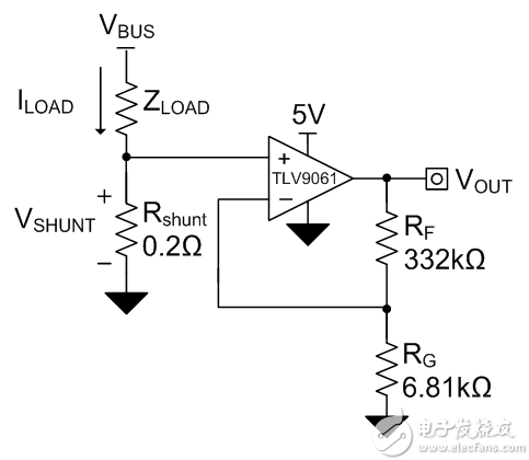
Figure 1: Low-side current sensing schematic
Equation 1 is to calculate the transfer function of the circuit shown in Figure 1:
among them.
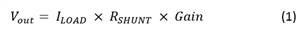
Accurate low-side current sensing design has two major requirements for the design of printed circuit boards. First, make sure that the shunt resistor (Rshunt) is connected directly to the amplifier's non-inverting input and RG's ground. This is commonly referred to as "Kelvin connection." If you do not use the Kelvin method, a parasitic resistance in series with the shunt resistor (Rshunt) is generated, causing the system to produce gain errors. Figure 2 shows the location of parasitic resistance in the system.
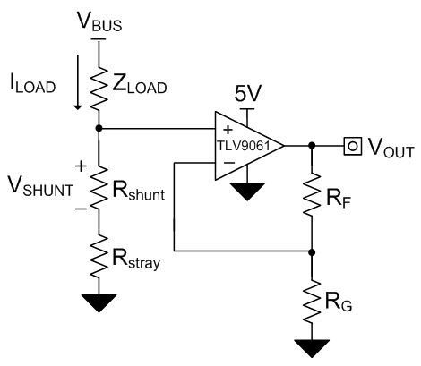
Figure 2: Parasitic resistance in series with a shunt resistor (Rshunt)
Equation 2 is to calculate the transfer function of the circuit in Figure 2:

The second design requirement is to place the ground of the resistor RG as close as possible to the ground of the shunt resistor (Rshunt). When the current flows through the ground plane of the printed circuit board, a voltage drop occurs in the ground plane, resulting in a difference in the voltage of the ground plane at different positions on the printed circuit board. This will make the system appear offset voltage. In Figure 3, the ground voltage source symbol connected to RG represents the difference in ground potential.
Figure 3: Difference in ground plane voltage
Equation 3 is to calculate the transfer function of the circuit shown in Figure 3:

Figure 4 shows the correct PCB layout.
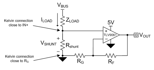
Figure 4: The correct layout
Figure 5 shows the printed circuit board layout that I suggested earlier for a low-side current-sensing design. The top layer is red and the bottom layer is blue. R5 and C1 in the printed circuit board layout indicate where the load resistance and decoupling capacitors should be placed.

Figure 5: Correct Low-Side Current-Sense PCB Layout
It should be noted that the trajectory from the shunt resistor (Rshunt) uses a Kelvin connection and RG is as close to the shunt resistor (Rshunt) as possible. You can use a small (0.8mm x 0.8mm) five-pin X2SON packaged TLV9061 op amp to place all passive components between the two pads of the top shunt resistor. From here, you can easily connect the bottom shunt resistor (Rshunt) line through the via to the top-phase inverting pin and RG.
When designing your printed circuit board layout for low-side current sensing in the future, it is important to follow these guidelines to reduce potential design errors:
Use a Kelvin connection on the shunt resistor (Rshunt).
Place RG as close as possible to the ground of the shunt resistor (Rshunt).
Decouple the capacitor as close as possible to the power pin.
There must be at least one reliable ground plane.
Outdoor Led Display,Outdoor Led Wall Display,Outdoor Led Walls,Outdoor Led Diigital Display
APIO ELECTRONIC CO.,LTD , http://www.displayapio.com