![<?echo $_SERVER['SERVER_NAME'];?>](/template/twentyseventeen/skin/images/header.jpg)
Cypress's FM4 S6E2C family is a highly integrated 32-bit MCU based on ARM® Cortex®-M4 with integrated flash and SRAM, as well as motor control timer, ADC and communication interface (USB, CAN, UART, CSIO (SPI) , I2C, LIN) peripherals, as well as hardware encryption engine (AES-128/192/256, SHA-256, PKA). Operating frequency 200MHz. This article introduces the main features and block diagram of FM4 S6E2C series, development board FM4-216- ETHERNE main features and block diagrams, circuit diagrams and PCB design drawings.
Devices in the S6E2CC Series are highly integrated 32-bit microcontrollers with high performance and compeTITIve cost. This series is based on the ARM Cortex-M4F processor with on-chip flash memory and SRAM. The serieshasperipherals such as motor control TImers, A/Dconverters, And communicates to the TYPE3-M4 product categories "FM4 Family Peripheral Manual Main Part (002-04856)."
The FM4 S6E2C-Series provides a highly integrated single chip solution with 200MHz of CPU power, up to 2Mbytes of dual banked high speed on chip flash memory, up to 256Kbytes of on chip SRAM, and integrated peripheral features including IEEE1588 compliant 10/100 base Ethernet, CAN, CAN-FD, USB and inverter control timers. The dedicated hardware cryptographic engine (AES-128/192/256, SHA-256, PKA) enables secure data communication with minimal CPU processing overhead.
Main features of FM4 S6E2C series:
32-bit ARM Cortex-M4F Core
ï® Processor version: r0p1
ï® Up to 200 MHz frequency operation
ï® FPU built-in
ï® Support DSP instructions
Memory protection unit (MPU): improves the reliability of an embedded system
ï® Integrated nested vectored interrupt controller (NVIC): 1 NMI (non-maskable interrupt) and 128 peripheral interrupts and 16 priority levels
ï® 24-bit system timer (Sys Tick): system timer for OS task management
On-chip Memories
ï® Flash memory
Thisseries isbased on two independent on-chip flashmemories.
ï¯ Up to2048 Kbytes
ï¯ Built-in flashaccelerator system with 16 Kbytes trace buffer memory
ï¯ Read access to flashmemorythatcan be achieved without wait-cycle up to an operatingfrequency of 72 MHz. Even at the operating frequency more than 72 MHz, an equivalent single cycle access to flashmemorycan be obtained by the flashaccelerator system.
ï¯ Security function for code protection
ï® SRAM
This is composed of three independent SRAMs (SRAM0, SRAM1 and SRAM2). SRAM0 is connectedto the I-code bus and D-code bus of Cortex-M4F core. SRAM1 and SRAM2 are connected to system bus ofCortex-M4F core.
ï¯ SRAM0: up to 192 Kbytes
ï¯ SRAM1: 32 Kbytes
ï¯ SRAM2: 32 Kbytes
External Bus Interface
ï® Supports SRAM, NOR, NAND flashand SDRAM device
ï® Up to 9 chip selects CS0 to CS8 (CS8 is only for SDRAM)
ï® 8-/16-/32-bit data width
ï® Up to 25-bit address bus
ï® Supports address/data multiplexing
ï® Supports external RDY function
ï® Supports scramble function
ï¯ Possible to set the validity/invalidity of the scramble function for the external areas 0x6000_0000 to 0xDFFF_FFFF in 4 Mbytes units.
ï¯ Possible to set two kinds of the scramble key
ï¯USB Interface (Max two channels)
The USB interface is composed of a function and a host.
ï® USB function
ï¯ USB2.0 Full-speedsupported
ï¯ Max 6 EndPoint supported
• EndPoint 0 is control transfer
• EndPoint 1, 2 can be selected bulk-transfer, interrupt-transfer or isochronous-transfer
• EndPoint 3 to 5 can select bulk-transfer or interrupt-transfer
• EndPoint 1 to 5 including double buffer
• The size of each endpoint is as follows.
−Endpoint0, 2to 5: 64byte
• EndPoint 1: 256byte
USB host
ï¯ USB2.0 Full-Speed/Low-Speedsupported
ï¯ Bulk-transfer, interrupt-transfer, and isochronous-transfer support
ï¯ USB Device connected/dis-connected automatically detect
ï¯ IN/OUT token handshake packet automatically
ï¯ Max 256-byte packetlength supported
ï¯ Wake-up function supported
CAN Interface (Max twochannels)
ï® Compatible with CAN specification 2.0A/B
ï® Maximum transfer rate: 1 Mbps
ï® Built-in 32-message buffer
CAN-FDInterface (Onechannel)
ï® Compatible with CAN Specification 2.0A/B
ï® Maximum transfer rate: 5Mbps
ï® Message buffer for receiver: up to 192 messages
ï® Messagebuffer for transmitter: up to 32messages
ï® CAN with flexible data rate(non-ISO CAN FD)
ï® Notes:
ï¯ CAN FD can communicate between non-ISO CAN FD and ISO CAN FD, because non-ISO CAN FD and ISO CAN FD are different frame format.
ï¯ About the problem of “non-ISO CAN FDâ€, see the White Paper from CiA (CAN in Automation).
Multi-function Serial Interface (Max16Channels)
ï® Separate 64 byte receive and transmit FIFObuffers for channels 0 to 7.
ï® Operation mode is selectable for each channel from the following:
ï¯ UART
ï¯ CSIO (SPI)
ï¯ LIN
ï¯ I2C
ï® UART
ï¯ Full-duplex double buffer
ï¯ Selection with or without parity supported
ï¯ Built-in dedicated baud rate generator
ï¯ External clock available as a serial clock
ï¯ Various error detect functions available (parity errors, framing errors, and overrun errors)
ï® CSIO (SPI)
ï¯ Full-duplex double buffer
ï¯ Built-in dedicated baud rate generator
ï¯ Overrun error detect function available
ï¯ Serial chip select function (ch 6 and ch 7 only)
ï¯ Supports high-speed SPI (ch 4 and ch 6 only)
ï¯ Data length 5 to 16-bit
ï® LIN
ï¯ LIN protocol Rev.2.1 supported
ï¯ Full-duplex double buffer
ï¯ Master/slave mode supported
ï¯ LINbreak field generation (can change to 13-to 16-bit length)
ï¯ LINbreak delimiter generation (can change to 1-to 4-bit length)
ï¯ Various error detect functions available (parity errors, framing errors, and overrun errors)
ï® I2C
ï¯ Standard mode (Max 100 kbps)/Fast mode (Max 400 kbps) supported
ï¯ Fast mode Plus (Fm+) (Max 1000 kbps, only for ch 3= ch A and ch 7=ch B) supported
DMA Controller (EightChannels)
DMA controller has an independent bus, so the CPU and DMA controller can process
Simultaneous
ï® Eightindependently configured and operated channels
ï® Transfer can be started by software or request from the built-in peripherals
ï® Transfer address area: 32-bit (4 GB)
ï® Transfer mode: Block transfer/Burst transfer/Demand transfer
ï® Transfer data type: bytes/half-word/word
ï® Transfer block count: 1 to 16
ï® Number of transfers: 1 to 65536
DSTC (Descriptor System Data Transfer Controller; 256 channels)
The DSTC can transfer data at high-speed without going via the CPU. The DSTC adopts the descriptor system and, following the specified contents of the descriptor thathas already been constructed on thememory, can access directly the memory/peripheral device and perform the data-transfer Operation.
It supports the software activation, the hardware activation and the chain activation functions.
A/DConverter (Max 32 Channels)
ï® 12-bit A/D Converter
ï¯ Successive approximation type
ï¯ Built-in threeunits
ï¯ Conversion time: 0.5μs at5V
ï¯ Priority conversion available (priority at two levels)
ï¯ Scanning conversion mode
ï¯ Built-in FIFO for conversion data storage (for SCAN conversion: 16steps, for priority conversion: 4steps)
D/A Converter (Maxtwochannels)
ï® R-2R type
ï® 12-bit resolution
Base Timer (Max 16channels)
Operation mode is selectedfrom the following for each channel:
ï® 16-bit PWM timer
ï® 16-bit PPG timer
ï® 16-/32-bit reload timer
ï® 16-/32-bit PWC timer
General Purpose I/O Port
This series can use its pins as general purpose I/O ports when they are not used for external bus or peripherals; moreover, the port relocate function is built in. It can set the I/O port to which the peripheral functioncan be allocated.
ï® Capable of pull-up control per pin
ï® Capable of reading pin level directly
ï® Built-in port-relocate function
ï® Up to 120high-speedgeneral-purpose I/O ports in 144-pin package
ï® Some pins 5V tolerant I/O.See “4. Pin Descriptions†and “5. I/O Circuit Type†for the corresponding pins.
Multi-function Timer (Max threeunits)
The multi-function timer is composed of the following blocks:
Minimum resolution: 5.00ns
ï® 16-bit free-run timer × 3 ch/unit
ï® Input capture × 4 ch/unit
ï® Output compare × 6ch/unit
ï® A/D activation compare × 6ch/unit
ï® Waveform generator × 3 ch/unit
ï® 16-bit PPG timer × 3 ch/unit
The following functionscan be used to achieve the motor control:
ï® PWM signal output function
ï® DC chopper waveform output function
ï® Dead time function
ï® Input capture function
ï® A/D convertor activate function
DT DTIF (motor emergency stop) interrupt function
Real-Time Clock (RTC)
The real-time clock can count year, month, day, hour, minute, second, or day of the week from 01 to 99.
Interrupt function with specified date and time (year/month/day/hour/minute/second/day of theweek) is available. This function is also available by specifying only year, month, day, hour, or minute.
ï® Timer interrupt function after set time or each set time.
ï® Capable of rewriting the time with continuing the time count.
ï® Leap year automatic count is available.
Quadrature Position/Revolution Counter (QPRC; Max fourchannels)
The Quadrature Position/Revolution Counter (QPRC) is used to measure the position of the positionencoder. It is also possible to use up/down counter.
Detection The detection edge of the three external event input pins AIN, BIN and ZIN is configurable.
ï® 16-bit position counter
ï® 16-bit revolution counter
ï® Two 16-bit compare registers
Dual Timer (32-/16-bit Down Counter)
The dual timer consists of two programmable 32-/16-bit down counters.Operation mode is selectable from the following for each channel:
ï® Free-running
ï® Periodic (= Reload)
ï® Oneshot
Watch Counter
The watch counter is used for wake up from low-power consumption mode. It is possible to select the main clock, sub clock, built-in High-speed CR clock, or built-in low-speed CR clock as the clock source.
ï® Interval timer: up to 64 s (max) with a sub clock of 32.768 kHz
External Interrupt Controller Unit
ï® External interrupt input pin: Max 32pins
Include Include one non-maskable interrupt (NMI)
Watchdog Timer (Twochannels)
A watchdog timer can generate interrupts or a reset when a time-out value is reached.
This series consists of two different watchdogs:a “hardware†watchdog and a “software†watchdog.
The hardware watchdog timer is clocked by low-speed internal CR oscillator. The hardware watchdog is thus active in any power saving mode except RTC mode and Stopmode.
Cyclic Redundancy Check (CRC) Accelerator
The CRC accelerator helps to verify data transmission or storage integrity.
CCITT CRC16 and IEEE-802.3 CRC32 are supported.
ï® CCITT CRC16 generator polynomial: 0x1021
ï® IEEE-802.3 CRC32 generator polynomial: 0x04C11DB7
Programmable Cyclic Redundancy Check (PRGCRC) Accelerator
The CRC accelerator helps a verify data transmission or storage integrity.
CCITT CRC16, IEEE-802.3 CRC32and generating polynomial are supported.
ï® CCITT CRC16 generator polynomial: 0x1021
ï® IEEE-802.3 CRC32 generator polynomial: 0x04C11DB7
ï® Generating polynomial
SD Card Interface
It is possible to use the SD card that conforms to the following standards.
ï® Part 1 Physical Layer Specification version 3.01
ï® Part E1 SDIO Specification version 3.00
ï® Part A2 SD Host Controller Standard Specification version 3.00
ï® 1-bit or 4-bit data bus
Ethernet-MAC
ï® Compliant with IEEE802.3 specification
ï® 10Mbps/100 Mbps data transfer rates supported
ï® MII/RMII for external PHY device supported.
ï® MII: Max one channel
ï® RMII: Max one channel
ï® Full-duplex and half-duplex mode supported.
ï® Wake-ON-LAN supported
ï® Built-in dedicated descriptor-system DMAC
ï® Built-in 2Kbytestransmit FIFO and 2Kbytesreceive FIFO.
ï® Compliant IEEE1558-2008 (PTP)
I2S (Inter-IC Sound Bus) Interface (TX x onechannel, RX x onechannel)
ï® Supportsthree transfer protocols
ï¯ I2S
ï¯ Left justified
ï¯ DSP mode
ï¯ Separate clock generation block for flexible system integration options
ï® Master/slave mode selectable
ï® RX Only, TX Only or TX and RX simultaneous operation selectable
ï® Word length is programmable from 7-bits to 32-bits
ï® RX/TX FIFO integrated (RX: 66 words x 32-bits, TX: 66 words x 32-bits)
DMA DMA, interrupts, or polling based data transfer supported
High-speed Quad SPI
Up to 66 MHz clock rates for very fast data transfers to and from SPI compatible devices.
Up to 256 Mbytes of memory mapped address space.
ï® Single data rate (SDR)
ï® Supportssingle,dual,and quad data modes
ï® Built-indirectmode and commandsequencermode
ï¯ Direct mode: Accessby use oftransmissionFIFO/reception FIFO(up to16word x 32bit)
ï¯ Commandsequencer mode: Automaticaccessassignedtoexternaldevice area.
Clock and Reset
ï® Clocks
Five clock sources (twoexternal oscillators, twointernal CR oscillators, and Main PLL) that are dynamicallyselectable.
ï¯ Main clock: 4MHz to 48MHz
ï¯ Sub clock: 30 kHz to 100 kHz
ï¯ High-speed internal CR clock: 4MHz
ï¯ Low-speed internal CR clock: 100kHz
ï¯ Main PLL Clock
ï® Resets
ï¯ Reset requests from INITX pin
ï¯ Power on reset
ï¯ Software reset
ï¯ Watchdog timer reset
ï¯ Low-voltage detector reset
ï¯ Clock supervisor reset
Clock Supervisor (CSV)
Clocks generated by internal CR oscillators are used to supervise abnormality of the external clocks.
ï® External OSC clock failure (clock stop) is detected, reset is asserted.
ï® External OSCfrequency anomaly is detected, interrupt or reset is asserted.
Low-Voltage Detector (LVD)
This series includes two-stage monitoring of voltage on the VCC pins. When the voltage falls below the voltage that has been set, the low-voltage detector functiongenerates an interrupt or reset.
LV LVD1: error reporting via interrupt
LV LVD2: auto-reset operation
Low-power consumption mode
Six lowpower consumption modes are supported.
ï® Sleep
ï® Timer
ï® RTC
ï® Stop
ï® Deep standby RTC (selectable from with/without RAM retention)
ï® Deep standby stop (selectable from with/without RAM retention)
Peripheral Clock Gating
The system canreducethe current consumption of the total system with gating the operation clocks of peripheral functionss not used.
VBAT
The consumption power during the RTC operation can be reduced by the power supply independent from the RTC (calendar circuit) / 32 kHz oscillation circuit. The following circuits can also beused.
ï® RTC
ï® 32-kHz oscillation circuit
ï® Power-on circuit
ï® Back up register: 32 bytes
ï® Portcircuit
Crypto Assist Function
These features are enabled for the crypto assist function. The dedicated middleware is necessary for this calculator operation.
ï® PKA (Public Key Accelerator)
ï¯ PKA (Public Key Accelerator) is modular exponentiation calculation accelerator used of RSA Public Key crypto and so on.
ï¯ Available bit length: Up to 2048-bit
ï® AES calculator
ï¯ AES (Advanced Encryption Standard) calculator is a AES common key crypto accelerator which is compliant with FIPS (Federal Information Processing Standard Publication) 197.
ï¯ Available key length: 128/192/256-bit
ï¯ CBC modeand ECB mode support
ï® SHA-256 calculator
ï¯ SHA-256 calculator is a SHA-256 hash function accelerator which is compliant with FIPS180-2.
ï® External Bus Data Scramble
ï¯ It enables to scramble input/output data of External Bus Interface.
Voice Function
These features are enabled for the voice function. Thededicated library is necessary for using the voice function.
ï® Automatic Speech Recognition (ASR)
ï¯ 100 custom commands in multiple languages
ï¯ User is defined with a text file (no audio input or training required)
ï® Natural Language Understanding (NLU)
Debug
ï® Serial wire JTAG debug port (SWJ-DP)
ï® Embedded trace macrocells (ETM) provide comprehensive debug and trace facilities.
AH AHB trace macrocells(HTM)
Unique ID
Unique value of the device (41-bit) is set.
Power Supply
ï® Five power supplies
ï¯ Wide range voltage: VCC= 2.7Vto 5.5V
ï¯ Power supply for USB ch 0 I/O: USBVCC0= 3.0V to 3.6V (when USB is used)
= 2.7V to 5.5V (when GPIO is used)
ï¯ Power supply for USB ch 1 I/O: USBVCC1= 3.0V to 3.6V (when USB is used)
= 2.7V to 5.5V (when GPIO is used)
ï¯ Power supply for Ethernet-MAC I/O: ETHVCC = 3.0Vto 5.5V(when Ethernet is used.)
= 2.7Vto 5.5V(when GPIO is used)
ï¯ Power supply for VBAT: VBAT= 1.65Vto 5.5V 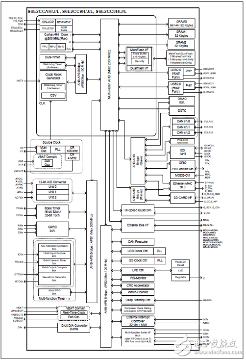
Figure 1. FM4 S6E2C Series Block Diagram
Development Board FM4-216-ETHERNE
The FM4-216-ETHERNET is a development platform for developing applications using the ARM® Cortex®-M4-based FM4 S6E2CC MCU. This board provides a variety of peripherals for evaluating different modules of the MCU, including Ethernet, CAN and USB Host .
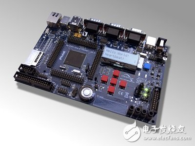
Figure 2. Development board FM4-216-ETHERNE outline drawing
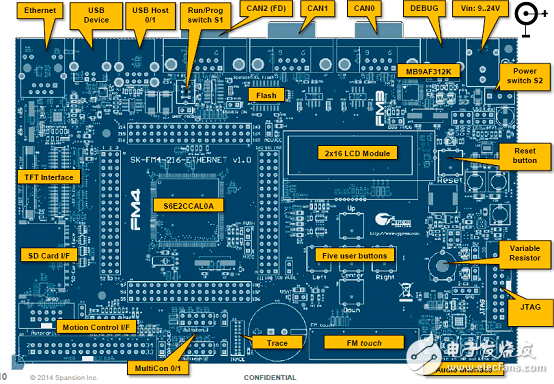
Figure 3. Main function distribution map of development board FM4-216-ETHERNE
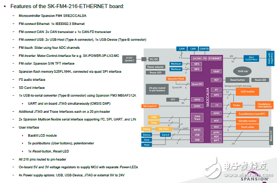
Figure 4. Main features and block diagram of the development board FM4-216-ETHERNE
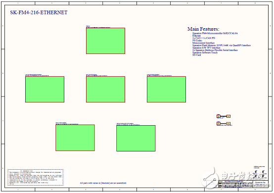
Figure 5. Development board FM4-216-ETHERNE circuit diagram (1)
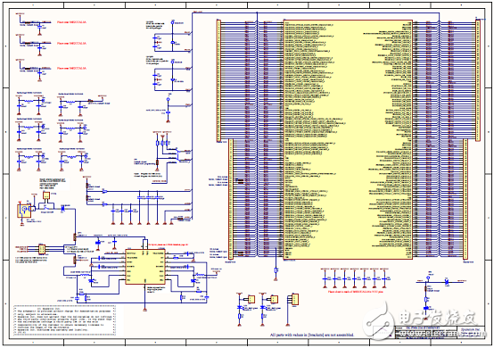
Figure 6. Development board FM4-216-ETHERNE circuit diagram (2)
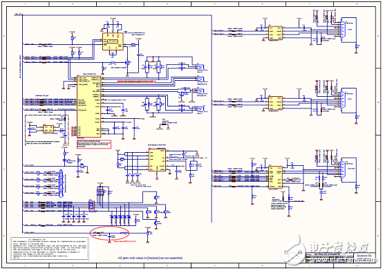
Figure 7. Development board FM4-216-ETHERNE circuit diagram (3)
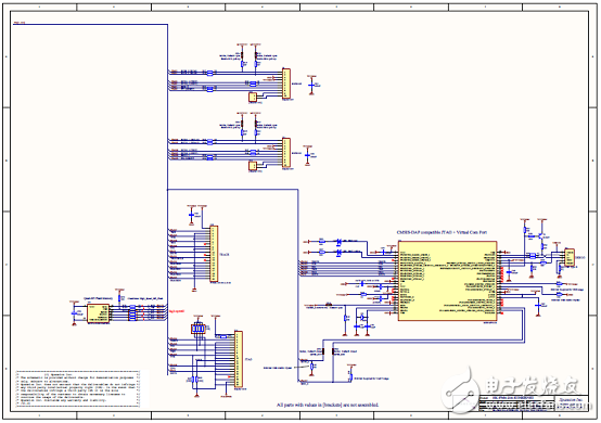
Figure 8. Development board FM4-216-ETHERNE circuit diagram (4)
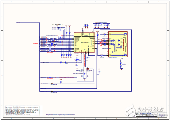
Figure 9. Development board FM4-216-ETHERNE circuit diagram (5)
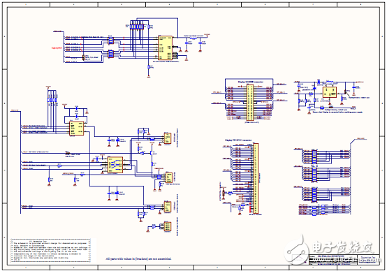
Figure 10. Development board FM4-216-ETHERNE circuit diagram (6)
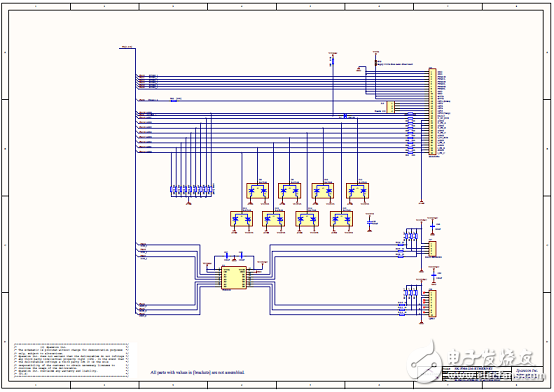
Figure 11. Development board FM4-216-ETHERNE circuit diagram (7)
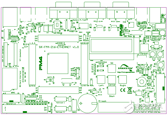
Figure 12. Development board FM4-216-ETHERNE PCB design (1)
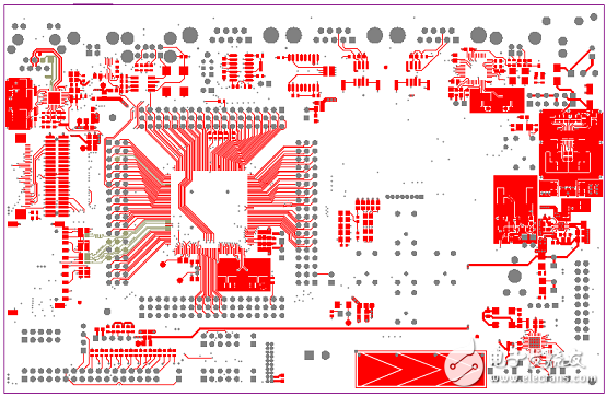
Figure 13. Development board FM4-216-ETHERNE PCB design (2)
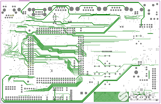
Figure 14. Development board FM4-216-ETHERNE PCB design (3)
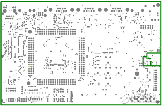
Figure 15. Development board FM4-216-ETHERNE PCB design (4)
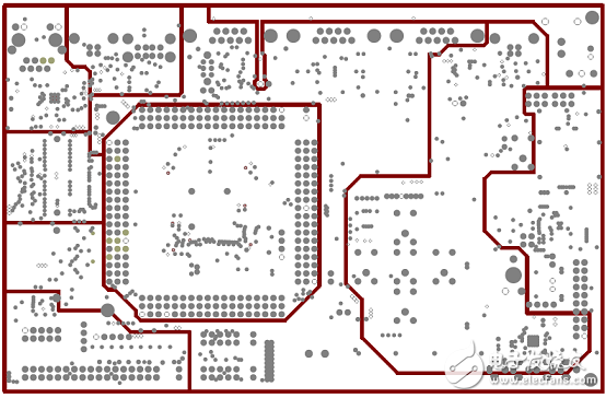
Figure 16. Development board FM4-216-ETHERNE PCB design (5)
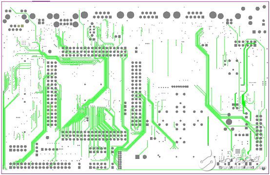
Figure 17. Development board FM4-216-ETHERNE PCB design (6)
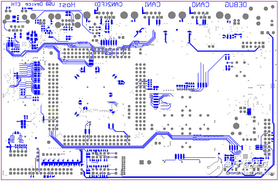
Figure 18. Development board FM4-216-ETHERNE PCB design (7)
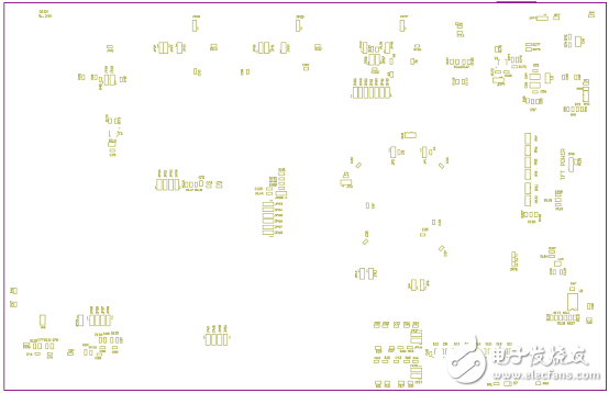
Figure 19. Development board FM4-216-ETHERNE PCB design (8)
Dash Mining Machine:Bitmain Antminer D7 (1286Gh),Baikal BK-G28,Baikal BK-X,Baikal Giant+ A2000,Innosilicon A5 DashMaster,iBeLink DM22G,Bitmain Antminer D3 (15Gh),StrongU STU-U6,Bitmain Antminer D5 (119Gh)
In short, Dashcoin Dash is a variant of the Bitcoin cryptocurrency that runs on the same blockchain network. Dashi, which combines the words "digital" and "cash," has become one of the most widely watched counterfeit coins in recent months. Originally released as "XCoin", it was later changed to "Darkcoin" and later Dash.
Arguably the biggest benefit of Dashi is that its transactions can be sent completely anonymously, just like legal cash payments. This is achieved by using a hybrid protocol that operates a dedicated network of servers called Masternodes. While Bitcoin operates only a single-layer network of miners, Dashcoin uses these master nodes as additional layers to its network, eliminating the need for a trusted third party to authorise a transaction that could compromise the anonymity of any payment.
Another major difference between Dashcoin and Bitcoin is that the former distributes mining rewards between its mining community, participants holding a specified amount of Dash, and the Dash community's long-term development fund.
Dash Miner,Dash Mining Machine,Bitmain antminer d7, D7 miner,X11 algorithm
Shenzhen YLHM Technology Co., Ltd. , https://www.ylhm-tech.com