![<?echo $_SERVER['SERVER_NAME'];?>](/template/twentyseventeen/skin/images/header.jpg)
As a non-polluting energy source, solar energy research has been a hot topic of research. In order to improve the energy conversion efficiency of solar energy, the research of photovoltaic grid-connected inverter is the focus of photovoltaic utilization. For photovoltaic grid-connected inverters, the topology can be divided into:
High-frequency transformer type, power frequency transformer type and transformerless type. The high-frequency transformer is small in size, light in weight and high in efficiency, but the control is complicated; the power frequency transformer is bulky, heavy, and simple in structure; in order to improve the efficiency and reduce the cost of the photovoltaic grid-connected system, it can be used when there is no special requirement. Transformerless topology. However, since there is no transformer, the input and output are not electrically isolated, and the parasitic capacitance of the photovoltaic array formed by the series and parallel connection of the photovoltaic modules becomes large, and the capacitance is greatly affected by the external environment, and the resulting common mode current will be large. For the study of leakage current, there are various solutions: when the full-bridge inverter adopts the unipolar modulation mode, there is a common mode voltage of the switching frequency pulsation, and when the bipolar modulation mode is adopted, the common mode The voltage is constant, and its amplitude is equal to half of the bus voltage; in the half-bridge inverter, the parasitic capacitance voltage to the ground is also clamped to the half of the bus voltage by the input voltage divider, which remains basically unchanged. These are methods based on bridge circuits to solve leakage current. In recent years, a double-buck inverter structure has emerged. This type of inverter has the characteristics of no bridge arm straight through, body diode not working, and bipolar operation. Therefore, it is widely used. This paper proposes a new three-level dual-buck inverter scheme, and sets the corresponding control strategy to achieve maximum power point tracking and grid-connected control.
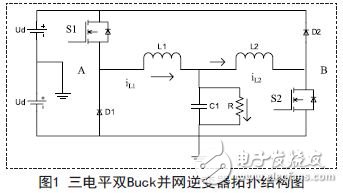
2. The overall solution of the three-level dual-buck inverterAs shown in Figure 1, the circuit topology of the dual-buck inverter, the dual-buck inverter uses a half-cycle mode. When the output current is in the positive half cycle, the power transistor S1, the freewheeling diode D1, and the filter inductor L1 and the filter capacitor Cf together form the Buck1 circuit. When the output current is negative half cycle, the power tube S2, the freewheeling diode D2, the filter inductor L2 and the filter capacitor Cf together form a Buck2 circuit, and the two Buck circuits do not work at the same time. Compared with the traditional bridge inverter circuit, the circuit has no bridge arm through, and the body diode does not need to participate in the working process. However, in this case, the voltages that the power tubes S1 and S2 are subjected to during the half cycle of operation are twice the DC bus voltage Ud. Since the voltage waveform output by the bridge arm itself is still bipolar, its harmonic content is still very large.
By optimizing the dual-buck inverter topology, the power switch on the original bridge arm is replaced by a combination of two power transistors and a fast recovery diode (ie S1 & S3 & D3 and S4 & S2 & D4). A new three-level dual-buck inverter topology as shown in Figure 2 is obtained.
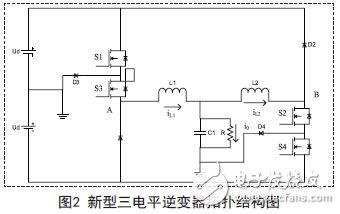
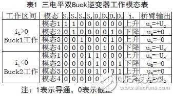
The new three-level dual-buck inverter is based on a half-cycle mode: when the output inductor current iL is positive half-cycle, the Buck1 circuit operates, and when the inductor current is negative half-cycle, the Buck2 circuit operates. The specific working modes are shown in Table 1. The optimized three-level dual-buck inverter has zero leakage current due to its parasitic capacitance voltage to ground being half of the input voltage.
In order to achieve maximum power point tracking and control of output voltage and current, the entire control uses a composite control strategy, including a voltage equalization control loop, a current control loop and a current reference loop as shown in Figure 3.
The specific work flow is: by collecting the voltage UC1 on the capacitor C1, calculating half of the bus voltage to obtain UZ=Ubus/2, respectively calculating the difference between UC1 and Uz, inputting the difference to the regulator of the voltage equalizing loop, and outputting the control current The amount of change Δi; the bus voltage is obtained through the maximum tracking link to obtain the reference current ig, the reference current iL is subtracted from the control current change amount Δi and the incoming current ig, and the last obtained current is subjected to a proportional integral error amplifying circuit to intersect the triangular wave. The control logic generates a preemptive pulse width modulation signal (SPWM wave), and the output SPWM waveform controls the on and off of the switch tube to realize the voltage adjustment function.
In the formula, c1 U and c2 U are the initial voltages of the capacitor C1 and the capacitor C2. If the two capacitor voltages are equal in magnitude, the deviation of the two capacitor voltages is:

For the above closed-loop system, set the parameters and simulate it. The specific parameters are set as follows: input DC voltage Ud=720V, input capacitance C1=C2=1100uF, output filter inductor L1=L2=750uH, expected output AC voltage Uo=220V, The frequency is 50Hz, and the rated output power Po=1KW.
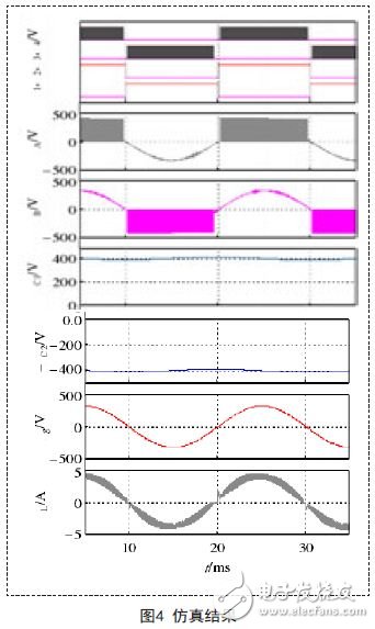
The specific simulation results are shown in Figure 4. ug is the grid voltage, iL is the inductor current, Uc1 is the voltage of capacitor C1, UC2 is the voltage of capacitor C2, and V1~V4 respectively represent the inverter for power switch S1~S4. Control signal. Specific working conditions: When iL is greater than zero, that is, working in the positive half cycle, the Buck1 circuit works, the power switch tubes S1, S3 are turned on, S2, S4 are turned off, iL2=0, at this time the voltage uB=ug; when iL is less than zero, That is, when working in the negative half cycle, the Buck2 circuit works, the power switch tubes S1, S3 are off, S2, S4 are on, iL2=0, at this time the voltage uA=ug, the closed loop system collects the capacitance signal to realize the input voltage equalization control, so The input capacitors UC1 and UC2 remain stable.
5. SummaryThis paper analyzes the topology of the traditional bridge inverter circuit and the new three-level double-buck inverter circuit, analyzes the leakage current of the common double-buck inverter circuit and proposes a new single-phase double-buck photovoltaic inverter. The improved three-level dual-buck inverter circuit voltage-clamps the parasitic capacitance between the inverter bridge arm and the ground through a voltage-dividing capacitor, and suppresses the leakage current for low frequency variations of the grid frequency. . A corresponding control strategy is developed for the new three-level dual-buck inverter circuit, and the maximum power tracking and voltage equalization control are realized by sampling the voltage signal. Finally, the correctness of the three-level double-buck inverter circuit is verified by the simulation waveform, and good experimental results are obtained.
High resolution
In order to realize a large-area high-resolution Liquid Crystal Display, it is usually necessary to use low-impedance metal materials, high-performance switching elements, and high-precision processing techniques. Aluminum is the most researched and used material for making TFT buses with low-impedance metals. By solving the problems of easy formation of hillocks, chemical corrosion and oxidation of aluminum, alloy methods (such as Al-Cu, Al-Si, Al-Nd and Al-Ti, etc.) and interlayer methods (such as Mo/Al/Mo) have been reported successively. , Cr/Al/Cr and Ti/Al/Ti, etc.), the alloy method is relatively simple in process, but the material has a higher resistivity. In May 1998, IBM developed a 16.3-inch ultra-high resolution (200ppi) a-Si TFT Display using Al-Nd alloy as the gate electrode, and mass production has been achieved. In April 1999, Toshiba introduced the 20.8-inch 16-SVGA (3, 200 × 2, 400) a-Si TFT-LCD, which can be said to represent the highest level of a-Si TFT-LCD in terms of high resolution and high capacity. .
According to Display Search in the third quarter of 2011, the global flat panel display research report "QuarterlyWorldw ide Flat Pane l Dis play Fore cas t Re port" pointed out that the average pixels per inch (ppi) in large-size LCD panels (>9.1 inches) ) Will grow from 88ppi in 2010 to 98ppi in 2015. The ppi of small and medium-sized LCD panels (<9.0 inches) will grow from 180ppi to 300ppi in the same period. With the rise of smart phones, mobile phones will be the most obvious application product for ppi's growth.
Another important way to realize high-resolution liquid crystal display is to develop LT p-Si TFT technology. The resolution of published p-SiTFT-LCD products is generally around 200ppi. Compared with a-Si TFT-LCD, LT p-Si TFT-LCD has a smaller volume of thin film transistors and storage capacitors. Therefore, it has a larger penetration area per inch, resulting in a brighter display. , And save more power. When the market demands higher ppi, low-temperature polysilicon (LTPS) technology becomes the best choice for manufacturing high-resolution thin-film transistor liquid crystal displays.
Contrast
The control ICs, filters and oriented films used in LCD manufacturing are related to the contrast of the panel. For general users, a contrast ratio of 350:1 is sufficient, but such contrast in the professional field does not satisfy users. Demand. Compared with CRT monitors easily reaching 500:1 or even higher contrast, only high-end LCD monitors can achieve this level. The first-tier LCD monitors on the market, such as Samsung, Asus, LG, etc., can reach a contrast ratio of 1000:1. However, because the contrast is difficult to accurately measure with instruments, you have to go and see it yourself when you pick it.
Tip: Contrast is very important. It can be said that the selection of LCD is a more important indicator than bright spots. When you understand that your customers buy LCDs for entertainment and watching DVDs, you can emphasize that contrast is more important than no dead pixels. We When watching streaming media, the brightness of the source is generally not large, but to see the contrast of light and dark in the scene of the character, the texture change from gray to black hair must be shown by the level of contrast. The 256-level grayscale in the test software In the test, more small gray grids can be seen clearly when looking up, which means that the contrast is better!a
Lcd Display Module,Tft Lcd Screen Display,Display Lcd Enclosure,Tft Display Lvds
ESEN Optoelectronics Technology Co., Ltd, , https://www.esenlcd.com