![<?echo $_SERVER['SERVER_NAME'];?>](/template/twentyseventeen/skin/images/header.jpg)
Hello, everyone, it's time to study everyday. Today we come to talk about the bus interface.
I. I2C bus The I2C bus is a serial bus introduced by PHLIPS. It is a high-performance serial bus with bus arbitration and high- and low-speed device synchronization required by a multi-master system. It uses two bidirectional I/O lines: SCL. (Serial clock line) and SDA (serial data line). The bus is mainly used to connect the overall circuit (ICS), I2C is a multi-directional control bus, that is to say a plurality of chips can be connected to the same bus structure, and each chip can be used as a control source for implementing data transmission. This simplifies the signal transmission bus. Master and slave can be linked to multiple slave devices. The internal SDA and SCL pin structure of each I2C bus device is the same. The pin's output drive is connected with the input buffer. The output is an open-drain FET and the input buffer is a high-input impedance non-inverting device. 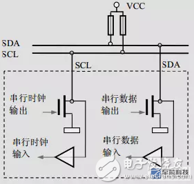
This circuit has two features:
(1) Since SDA and SCL are open-drain structures, the "line sum" logic of the signal is realized by means of an external pull-up resistor;
(2) The pin will detect the level on the pin at the same time as the output signal, and check whether it is consistent with the output just now. Provides hardware infrastructure for "clock synchronization" and "bus arbitration."
If the slave wants the host to reduce the transfer speed, the host can be notified by actively pulling the SCL low for a longer time. When the master waits for the next transfer and the SCL level is pulled low, it waits until the slave. Complete the operation and release control of the SCL line. In this way, the host is actually controlled by the clock synchronization of the slave. It can be seen that the low level on the SCL line is determined by the device with the longest clock low; the high time is determined by the device with the shortest high time. This is clock synchronization, which solves the speed synchronization problem of the I2C bus.
Second, SPI bus SPI (Serial Peripheral Interface - serial peripheral interface) bus system is a synchronous serial peripheral interface, which allows the MCU and various peripheral devices to communicate in a serial manner to exchange information. This interface generally uses 4 lines. The three registers of SPI are: control register SPCR, status register SPSR, data register SPDR.
The SPI interface is a synchronous serial data transmission between the CPU and the peripheral low-speed devices. Under the master device's shift pulse, the data is transmitted bit by bit. The high bit is first and the low bit is the last bit. It is full duplex communication and the data transmission speed is overall. It is faster than the I2C bus and can reach several Mbps. 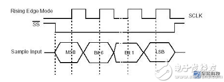
(1) MOSI - Master Data Output, Slave Data Input (2) MISO - Master Data Input, Slave Data Output (3) SCLK - Clock Signal, Generated by Master, Up to fPCLK/2, Slave Mode Frequency The maximum is fCPU/2
(4) NSS - Slave enable signal controlled by the master device, and some ICs will be marked as CS (Chip select)
In point-to-point communication, the SPI interface does not require addressing and is full-duplex communication, which is simple and efficient. In a multi-slave system, each slave requires an independent enable signal and is slightly more complicated in hardware than the I2C system.
The internal hardware of the SPI interface is actually two simple shift registers. The transmitted data is 8 bits. In the master device, the slave enable signal and the shift pulse are transmitted in bit-by-bit mode. The high bit is first and the low bit is low. . The data changes on the rising edge of SCLK while one bit of data is stored in the shift register.
SPI has four operating modes. CPOL and CPHA can be either 0 or 1 respectively:
CPOL: (Clock Polarity), clock polarity. When CPOL is 0, the level is low when the clock is idle; when CPOL is 1, the level is high when the clock is idle.
CPHA Clock Phase), clock phase. When CPHA is 0, the rising edge of the clock collects data, and the falling edge of the clock cycle outputs the data. When CPHA is 1, the falling edge of the clock collects data, and the rising edge of the clock cycle outputs the data.
Third, RS232, RS422, RS485 bus RS232: By the electronic industry association (Electronic Industries Association, EIA) developed by the asynchronous transmission standard interface. Usually the RS-232 interface appears as a 9-pin (DB-9) or 25-pin (DB-25) type. There are usually two sets of RS-232 interfaces on the personal computer. They are called COM1 and COM2 respectively. . It defines the serial connection between data terminal equipment (DTE) and data communication equipment (DCE). Serial communication interface standard.
RS-422: Balanced voltage digital interface circuit. Connect multiple receiving nodes on the same transmission line, and connect up to 256 nodes. That is, one Master and the rest Slave. RS-422 supports point-to-multipoint two-way communication. It is a parallel communication interface standard.
RS485: It is a two-wire system (used in shielded twisted pair). Is the master-slave communication mode, that is, a host with multiple slaves. In many cases, the RS-485 communication link is simply connected to the "A" and "B" sides of each interface using a pair of twisted pairs. The RS485 interface connector uses DB-9's 9-pin connector and DB-9 (hole) for the RS485 interface of the smart terminal and the DB485 (pin) for the keyboard interface of the keyboard.
RS232, RS422, RS485 difference:
a. Different communication distances:
1. RS232 can transmit up to 15 meters.
2. RS-422 is differential mode transmission, strong anti-interference ability, can transmit 1200 meters.
3. The maximum communication distance of RS485 is about 1219m.
b. The difference in logical representation:
1. RS232 uses -12V for logic 1, 12V for 0, full duplex, and at least 3 communication lines (RX, TX, GND), because absolute voltage is used for logic, because of interference, wire resistance and other reasons, the communication distance is not far .
2.RS422, using TTL differential level representation logic, is the two voltage differential representation logic, RS422 is defined as full duplex, so at least 4 communication lines (generally an extra ground wire), a driver It can drive up to 10 receivers (that is, the receiver is 1/10 unit load). The communication distance is related to the communication speed. Generally, the communication can be performed at a high rate when the distance is short, and long distance communication can be performed when the rate is low.
3.RS485, most of the inherited 422, the main difference is that RS485 can be half-duplex, and a driver's drive capability can drive at least 32 receivers (ie, the receiver is 1/32 unit load) when used Higher receivers can drive more receivers. So now most full-duplex 485 driver/receiver pairs are standard: RS422/485, because full-duplex RS485 driver/receiver pair can be used in RS422 network.
Fourth, USB
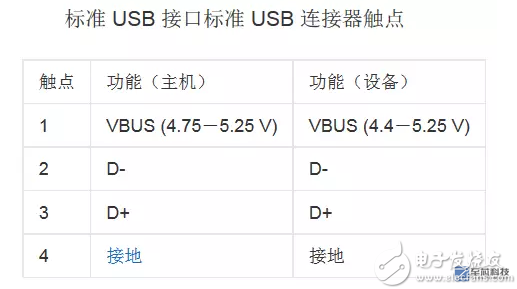
USB, which stands for Universal Serial Bus in English, is an external bus standard that regulates the connection and communication between computers and external devices. It is an interface technology applied in the PC field. The USB interface supports plug and play and hot plugging of the device. USB is a unified transmission specification, but there are many types of interfaces. The most common type is the flat type used on our computers. This is called type A, and there are four connections inside, according to who plugs into who The female interface is generally male with the male mouth and the female mouth is on the machine. USB signals are transmitted using twisted pairs labeled D+ and D-, respectively, and they each use a half-duplex differential signal and work cooperatively to cancel electromagnetic interference from long wires.
USB1.1 is a relatively common USB specification. Its high-speed transmission rate is 12Mbps, low-speed transmission rate is 1.5Mbps (b is bit), and 1MB/s (megabytes/second) = 8MBPS (megabits). /s), 12Mbps = 1.5MB/s. Currently, most MP3s are such interface types.
The USB2.0 specification evolved from the USB1.1 specification. Its transmission rate has reached 480Mbps, converted to MB is 60MB/s, enough to meet the speed requirements of most peripherals. The Enhanced Host Controller Interface (EHCI) in USB 2.0 defines an architecture that is compatible with USB 1.1. It can drive USB 1.1 devices with USB 2.0 drivers. In other words, all USB 1.1-capable devices can be used directly on the USB 2.0 interface without having to worry about compatibility issues, and accessories such as USB cables, plugs, etc., can also be used directly.
V. PCI
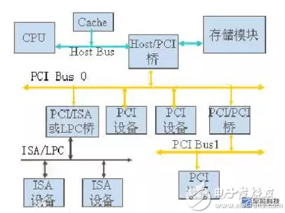
PCI, the Peripheral Component Interconnect, is a local parallel bus standard. It was developed from ISA bus. From a structural point of view, PCI is a bus that is inserted between the supplier of the CPU and the original system bus. Specifically, a bridging circuit manages this layer and implements an interface between the upper and lower interfaces to coordinate data transmission. .
The PCI bus is a tree structure that is independent of the CPU bus and can operate in parallel with the CPU bus. PCI devices can be connected to PCI devices and PCI bridges. Only one PCI master device is allowed on the PCI bus. The others are PCI slave devices. The read and write operations can only be performed between master and slave devices. The data exchange needs to transit through the master device. PCI bus structure as shown below.
The PCI bus is a synchronous, processor-independent 32-bit or 64-bit local bus with a maximum operating frequency of 33 MHz, a peak speed of 132 MB/s at 32-bit, and 264 MB/s at 64-bit. The bus specification was issued by PCISIG. . Compared with ISA bus, PCI bus has the following remarkable features:
(1) High-speed PCI local bus operates with a clock frequency of 33MHz. Using a 32-bit data bus, the data transfer rate can be as high as 132MB/s, which is far more than any of the previous buses. In addition, the master of the PCI bus can directly exchange data with the memory of the microcomputer.
(2) Plug and Play PCI hardware resources of the card are uniformly allocated by the microcomputer according to their respective requirements. There will never be any conflict.
(3) Reliability Compared with the ISA bus, which is commonly used in microcomputers, the PCI bus adds reliability measures such as parity check error (PERR), system error (SERR), and end-of-line (STOP) control signals, and timeout processing. The reliability of data transmission is greatly increased.
(4) Complexity The powerful functions of the PCI bus greatly increase the difficulty of hardware design and software development. On the hardware, a large-capacity, high-speed CPLD or FPGA chip is used to implement the complex functions of the PCI bus. On the software, a plug-and-play functional-enzyme device driver program is created using software tools based on the operating system used.
(5) Automatic configuration When the PCI card is inserted into the system, the BIOS will allocate the storage address, interrupt, and certain timing information for the card based on the information read about the card and the actual situation of the system.
(6) Shared interrupts The PCI bus is an active-low method. Multiple interrupts can share an interrupt line, while the ISA bus is an edge trigger.
(7) Good scalability Since PCI is designed to support the existing expansion bus standard, it is fully compatible with ISA, EISA and MCA buses.
(8) Multiplexing In order to optimize the design in the PCI bus, the address lines and the data lines share a set of physical lines, ie multiplexes. The PCI connector is small in size and uses multiplexing technology, which reduces the number of components and pins and improves efficiency.
(9) Strictly regulated The PCI bus has strict rules on protocol, timing, electrical performance, and mechanical performance, which ensures the reliability and compatibility of PCI.
Six, PCIE
PCI-Express (peripheral component interconnect express) is a high-speed serial computer expansion bus standard.
Conceptually, the PCI Express bus is a high-speed serial replacement for the older PCI/PCI-X bus. One of the main differences between PCI Express bus and old PCI is the bus topology. PCI uses a shared parallel bus architecture in which the PCI host and all devices share a common set of addresses, data, and control lines. In contrast, PCI Express is based on a point-to-point topology where a separate serial link connects each device to the root system (host). Due to its shared bus topology, the PCI bus in a single direction can be arbitrated (in the case of multiple hosts) and limited to one host at a time. In addition, the old PCI clocking scheme limited the bus clock to the slowest peripheral on the bus (regardless of the devices involved in the bus transaction). In contrast, PCI Express bus links support full-duplex communication between any two endpoints, while there are no inherent limitations on concurrent access across multiple endpoints.
In terms of the bus protocol, PCI Express communications are encapsulated in data packets. The work of packing and unpacking data and status message traffic is handled by the transaction layer of the PCI Express port. Fundamental differences in electrical signals and bus protocols require the use of different mechanical form factors and expansion connectors (therefore, new motherboards and new adapter boards are required ); PCI slots and PCI Express slots are not interchangeable.
At the software level, PCI Express retains backward compatibility with PCI; traditional PCI system software can detect and configure newer PCI Express devices without explicitly supporting the PCI Express standard, but the new PCI Express functionality cannot be accessed. The PCI Express link between the two devices can consist of 1 to 32 channels. In multi-channel links, packet data is striped across channels, and peak data throughput is proportional to the overall link width. The channel count is automatically negotiated during device initialization and can be limited by either endpoint.
PCI Express operates in consumer, server, and industrial applications as motherboard-level interconnects (connecting motherboard peripherals), passive backplane interconnects, and expansion card interfaces as add-on boards. Main applications: External GPUs, storage devices, cluster interconnects.
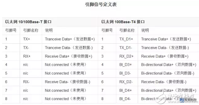
Seventh, network mouth The network mouth is the network high speed development has entered the G era. It is mainly divided into Gigabit Ethernet ports and Fast Ethernet ports. The Gigabit Ethernet ports are downward compatible, and the 100M Ethernet ports can also be connected.
RJ45 interface is a commonly used Ethernet interface, supporting 10 megabits and 100 megabits of adaptive network connection speed. RJ45 type network cable plug is also called crystal head. It is made of a total of eight cores and is widely used in network devices between LAN and ADSL broadband Internet users. Network cable (called CAT5 or Twisted Pair) connection. In the specific application, RJ45 type plug and network cable have two connection methods (line sequence), respectively called T568A line sequence and T568B line sequence.
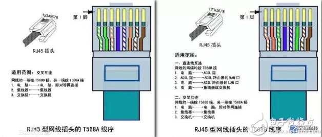
There are two types of common RJ45 interfaces: DTE (Data Terminal Equipment) types for Ethernet network cards, router Ethernet interfaces, and DCE (Digital Communication Equipment) types for switches. When two devices of the same type use the RJ45 interface to communicate, a crossover cable must be used. If the DTE type interface and the DTE type interface are connected without connecting pins, the touched pins are data receiving (transmitting) pins and communication cannot be performed. In addition: Some DCE type devices will automatically negotiate with each other. At this time, the connection can use straight lines or parallel lines.
Inverter Shell,Mini Inverter Shell,Best Inverter Shell,Hybrid Inverter
Original Electronics Technology (Suzhou) Co., Ltd. , https://www.original-te.com