![<?echo $_SERVER['SERVER_NAME'];?>](/template/twentyseventeen/skin/images/header.jpg)
The overall implementation scheme of FPGA-based video surveillance system is proposed. Firstly, the I2C bus configuration module is designed in FPGA to make a reasonable configuration of the video processing chip, and then the video signal processing process is briefly introduced. The processed video signal is stored in the SDRAM buffer through the ping-pong mechanism, and finally sent to the display for normal display according to the timing of the VGA. This design uses VerilogHDL language to write programs, and uses Modelsim software to simulate, using ISE to download to Virtex-II XC2VP30 FFG896 development board to achieve video surveillance.
A typical video surveillance system generally consists of a light source, a camera, a video conversion unit, a digital image transmission processing and control system, an input/output unit, and a monitor. The existing video surveillance system is mainly composed of industrial computer and video image acquisition card, which has the disadvantages of poor system stability and high price. Evolving FPGAs have the advantages of short design cycle, flexibility, and improved system reliability and integration. Verilog HDL language is similar to C language, flexible and easy to use. This paper combines the advantages of both to propose FPGA-based video. surveillance system. 1 System module division Most of the design work of the video surveillance system of this design is focused on the programming development of FPGA. Through analysis, the system can be divided into the following five functional modules, as shown in Figure 1.
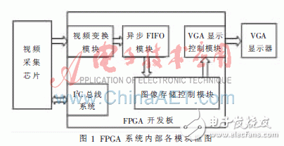
(1) Video interface module: The video capture chip has multiple acquisition modes. In this design, the FPGA configures its internal registers through the I2C bus to sample according to a certain format. (2) Video conversion module: Decode the obtained video stream, identify the line and field synchronization signals, and select the size of the acquired image according to the need, and then convert the image data into RGB format for subsequent display. (3) Asynchronous FIFO module: Since the video processor and SDRAM work at different clock frequencies, there will be a mismatch between read and write speeds. The solution is to add an asynchronous FIFO between the two. (4) Image storage module: The decoded data is sequentially stored in two SDRAMs via a ping-pong mechanism, and each SDRAM stores an image, and the two storage areas are alternately stored and input and outputted through the ping-pong mechanism, avoiding waiting ,accelerate. (5) VGA control module: According to the industrial parameters of VGA, generate the corresponding line synchronization signal and place synchronization signal, and send it to VGA for display at the appropriate time.
2 System module specific design 2.1 Video acquisition module
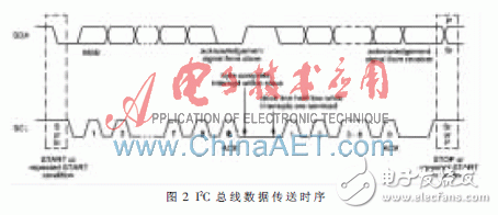
The video acquisition chip SAA7113 can convert 4 channels of input to its internal registers through the I2C bus. The input can be 4 channels of CVBS or 2 channels of S-video (Y/C) signals, and output 8 bit "VPO" bus, which is standard. ITU 656, YUV 4:2:2 format. The I2C bus system consists of two bus SCL (serial clock) and SDA (serial data) lines. The I2C bus transmission process consists of four parts: the start signal, the transmission header, the transmission data, and the end signal. The entire module can be divided into four states: normal state, waiting for ACK state, write data state, and end state. The I2C bus data transfer timing is shown in Figure 2.
2.2 Video Transformation Module The video conversion module decodes the obtained digital video stream, recognizes the line and field synchronization signals, and converts the YUV data format into image data in RGB format for subsequent display. 2.2.1 ITUR 656 Decoding The PAL system has 625 lines per frame, of which 572 lines are valid image data, and the other are field blanking signals; each line of image data contains 720 pixels. Therefore, the resolution of the PAL television signal is 720 & TImes; 572. The PAL television signal scans 25 frames per second, and each frame includes odd and even two fields of image. The 1-frame image is divided into an odd field and an even field, each having 286 lines of effective images.
The data format output by SAA7113 is standard ITU.656, YUV 4:2:2 video data. The luminance signal of each pixel occupies 8 bits, and the two chrominance signals occupy a total of 16 bits. Each pixel has its own luminance data Y, but every two adjacent pixels in the output data share a set of color difference data Cb, Cr. The data structure of each line of ITU656 is shown in Figure 3. Each line of data contains a horizontal control signal and a YCbCr video data signal. The video data words are transmitted at a rate of 27 MB/s in the order: Cb, Y, Cr, Y, Cb, Y, Cr, .... The 288 B at the beginning of each line is the line control signal, the EAV signal means the end of the active video, and the SAV signal means the effective video start.
2.2.2 YUV4: 2:2 is converted to YUV4:4:4 YUV4:2:2 is converted to YUV4:4:4 is mainly to convert serial data into parallel data, and YCbCr (4:2:2) video data Interpolation is performed to obtain YCbCr (4:4:4) video data, which is divided to obtain a pixel clock of 13.5 MHz.
2.2.3 Chroma space conversion
The color space transformation formula is: R=1.164(Y-16)+1.596(Cr-128) G=1.164(Y-16)-0.813(Cr-128)-0.392(Cb-128) B=1.164(Y-16 )+2.017(Cb-128)
2.3 asynchronous FIFO module
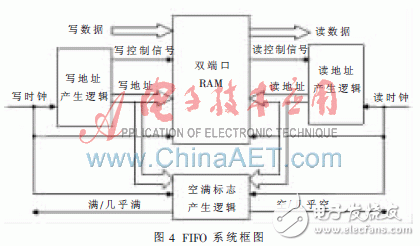
The FIFO is a FIFO memory that is primarily used to buffer data and isolate clock or phase differences. It uses a dual port memory to store data, the data sender writes data at one end, and the receiver reads the data at the other end. First, we need to use the RAM resources of the FPGA to instantiate a dual-port RAM. It needs to read and write at the same time, so that its input and output and depth are set according to the design requirements. The FIFO controller has reset, input and output data, and read. Write clock, read and write enable, and empty flag ports. The design principle block diagram is shown in Figure 4.
2.4 SDRAM Control Module 2.4.1 Introduction to the Principle of SDRAM Operation
A SDRAM contains several BANKs, and each BANK's memory cells are addressed in rows and columns. Due to this special memory structure, the working principle of SDRAM has the following characteristics: (1) After power-on of 100 μs~200 μs, the SDRAM mode register must be configured by an initialization process, and the mode register determines the working mode of the SDRAM; (2) SDRAM memory cell can be understood as a capacitor, always tend to discharge, so there must be a timing refresh cycle to avoid data loss, the refresh cycle can be calculated by the minimum refresh cycle + clock cycle; (3) SDRAM specific control Commands are assisted by some dedicated control pins and addresses.
2.4.2 SDRAM controller overall design
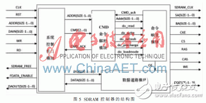
A schematic diagram of the interface between the SDRAM controller and the external is shown in FIG. 5. The left end interface signal of the controller is the system control interface signal connected to the FPGA, and the right end interface signal is a signal directly connected to the corresponding pin of the DSRAM. According to each interface signal, timing requirement and working mode of the SDRAM, the internal of the SDRAM controller is further refined into a plurality of functional modules, including a system control interface module, a CMD command parsing module, a command response module, and a data path module. The system control interface module is configured to receive a control signal of the system, thereby generating different CMD command combinations; the CMD command parsing module is configured to receive the CMD command and decode into an operation instruction; the command response module is configured to receive the operation instruction and generate an operation operation of the SDRAM; The data path module is used to control the effective input and output of data.
2.5 VGA Control Module 2.5.1 Video Digital to Analog Converter FMS3818
The FMS3818 is a low cost video digital-to-analog converter (DAC) that can accommodate graphics and video applications with a maximum pixel clock of 180 MHz. The VGA_OUT_BLANK_Z signal input covers the RGB input and the blank display output. When the FPGA does not program the XSGA output, this signal is left blank by the pull-down resistor and does not need to be controlled by the user.
2.5.2 Introduction to VGA Standard
VGA is a standard display interface that uses a progressive scan to project an image onto the screen. The standard VGA display has a field rate of 60 Hz and a line rate of 31.5 kHz. The horizontal timing includes several timing parameters of the horizontal pulse width, the width between the end of the horizontal sync pulse and the start of the horizontal gate, and the width of a complete video line. Vertical timing is similar to horizontal timing, including the vertical sync pulse width, the width between the end of vertical sync to the beginning of the vertical gate, the width of the visible area of ​​a video frame, and the width of a complete video frame.
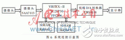
3 system hardware connection
The camera collects the light source signal, and the FPGA sends control information to the SAA7113 through I2C, so that it is sampled according to a certain format, converted into RGB format, stored in the SDRAM through the FIFO buffer, and finally sent to the VGA display through the video digital-to-analog converter FMS3818 for display. . The system hardware connection diagram is shown in Figure 6.
The design uses a top-down analysis method to analyze each functional module of the system according to the functional requirements of the system, and then specifically design each module. Combining digital video technology with FPGA design theory, using Verilog HDL language, the system has the advantages of flexible design and easy modification. At the same time, it can cooperate with other CPUs to complete further design. For example, adding certain algorithms can realize corresponding pattern recognition and other tasks. .
Plastic Capillary Pressure Gauge
Plastic Capillary Pressure Gauge,Mini-Sized Capillary Manometer,D28 Plastic Tube Pressure Gauge,Pipe Manometer
ZHOUSHAN JIAERLING METER CO.,LTD , https://www.zsjrlmeter.com